Both physical and chemical deposition play a large role in many popular industries today.
 Thin film evaporation and deposition is essentially the application of an extremely thin film of material – relative to the size of a few atoms – onto what is known as a “substrate” surface. It is then coated with a specific material that is chosen by the operator to form layers. The process of thin film deposition is an integral part of today’s semiconductor industries, solar panel production, CD manufacturing, and other optical device industries.
Physical and Chemical Deposition
Thin film deposition is divided into two categories – physical deposition and chemical deposition. Although they may sound similar, they have significant differences that allow them to perform tasks that the other cannot.
Chemical deposition utilizes a fluid precursor to produce a chemical change on a surface – resulting in a chemically deposited coat. An example of this is chemical vapor deposition which produces a high-purity, high-quality solid material that is used in the semiconductor industry today.
Physical deposition on the other hand, refers to a more broad range of technologies where a specific material is released from a designated source and deposited onto a substrate through the use of a mechanical, thermodynamic, or electromechanical process. Two of the most common techniques of physical vapor deposition are sputtering and evaporation – two methods that differ from each other due to their unique step-by-step processes.
Thermal Evaporation
The process of thermal evaporation involves the heating of a solid material that coats a substrate within a high vacuum chamber until it begins to boil and evaporates, therefore producing high vapor pressure. Now, inside this vacuum chamber, even a small amount of vapor pressure is enough to produce a cloud of vapor. This now evaporated material creates a stream that can travel through the vacuum environment without reacting or affecting the other atoms within the chamber. It will then travel all the way until it hits the substrate, thus “sticking” onto it as a thin film or coating.
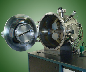
Sputtering
The process of sputtering is essentially the bombardment of a target material with a high amount of high-energy particles. Typically it’s used as a deposition method on a substrate for silicon wafers or solar panels. These substrates that are going to be coated are placed within a vacuum chamber that contains an inert gas. A negative electric charge is then utilized on the material that is going to be deposited, which then forces the plasma within the chamber to glow. The atoms are then sputtered off of the target through high-impact collisions with the inert gas, carrying these particles throughout the sputtering systems and then ultimately ending up being deposited as a thin film.
Denton Vacuum, LLC manufactures the finest ion beam sputter deposition equipment on the market. For questions on how you can go about purchasing these products, visit Denton Vacuum, LLC online today.