 Leonard Blavatnik is one of the richest men in Britain but is also a well-known philanthropist.
The Ukrainian-born American has an estimated net worth of $18.5 billion. Although Blavatnik is known for his donations, the philanthropist carefully chooses his beneficiaries. Often beneficiaries will include universities that have clear plans and progress reports on how his funding is used.
Blavatnik came from a Jewish family and was born in 1957 in Russia. He immigrated to America in 1978 and completed a Masters in computer science from Columbia University and an MBA from Harvard Business School.
The industrialist then founded Access Industries in 1986, which was an International conglomerate with strategic investments in the US and Europe. The company’s success was due to strategic, timely investments in post-Soviet aluminum and energy companies.
He then moved into chemicals by owning a stake in LyondellBasell Industries, which is one of the world’s leading chemical companies. He broadened his reach by investing in the Warner Music Group, which has now signed on many upcoming artists.
Blavatnik soon created the Blavatnik Foundation, which supports many cultural, art and academic institutions.
The foundation has since supported the British Museum, Tate Modern, the Prince’s Trust, the Royal Opera House, the Metropolitan Museum of Art, the National Gallery of Art, the National Portrait Gallery, and the Royal Academy of Art.
Apart from this, the foundation has created the Blavatnik Awards for Young Scientists which assist scientist with promising inventions.
Written by Access Industries. Len Blavatnik is a philanthropist who owns the international conglomerate and who also runs the Blavatnik Foundation.
 The application of diamond like carbon, or DLC, coatings has introduced a new way of producing high quality and consistent coatings for a variety of industries. This type of technology allows for deposition in large scale production machines without having to sacrifice film quality.
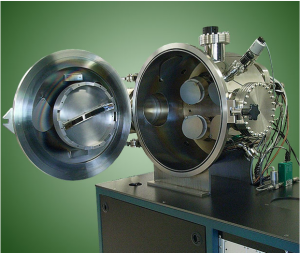 Thin film evaporation and deposition is essentially the application of an extremely thin film of material – relative to the size of a few atoms – onto what is known as a “substrate” surface. It is then coated with a specific material that is chosen by the operator to form layers. The process of thin film deposition is an integral part of today’s semiconductor industries, solar panel production, CD manufacturing, and other optical device industries.
 One of the biggest challenges the global community faces in the coming decades is how to solve the fundamental problem of energy consumption. As expert
  When preparing your big move across the country, one thing you may dread moving is your safe. This should be unsurprising since safes should be difficult to move to deter burglars. However, you will need to have a great plan for moving your safe across the country.
 In order to financially justify the implementation of an EDI system, a thorough cost analysis needs to be done. That cost will depend on which type of EDI system you go with, an in-house system, or with the use of an EDI service provider. Here are a look at the two systems: